
De-layered PCB Display
by kbembedded
25 January 2020Ever wondered how multi-layer PCBs fit together? Ever been curious about how PCBs are reverse engineered? In this project, we’ve torn down two different PCB designs to demonstrate a destructive method for de-layering multi-layer PCBs for further analysis, as well as encapsulating them for display.
More awesome photos of the final product at the end of the post.
Special Thanks
Before getting to the meat of this project, we have a couple of thanks to give out (in alphabetical order):
-
[Anonymous Friend] Thanks to [Friend] to opening his shop to me, providing his experience, knowledge, and skills of metal and woodworking. It was an interesting journey for both of us having never quite dealt with fiberglass and copper in this way.
-
Joe Grand (https://twitter.com/joegrand) Thanks to our friend, Joe Grand, for providing us with a pile of 4 layer PCBs that were all of the same rev. This allowed us to destroy a number of them and still be able to create the final displays.
-
Alvaro Prieto (https://twitter.com/alvaroprieto) Thanks to Alvaro for providing us with silicone moulds that were used to do the encapsulation of the final displays. We happened to spot a tweet from him while we were working out how to make the final displays. Said tweet was showcasing custom drink coasters that were PCBs encapsulated in resin. A discussion led to him sending the moulds he used my way, as well as shared experiences with casting resin.
Additionally, the book “PCB-RE: Tools & Techniques” was used as a loose guide for the process of de-layering. In my opinion, it is overall a great read for reverse engineering PCBs.
Why?
PCB reverse engineering plays a crucial role in completely understanding an electronic device. It allows for reconstructing the original schematic used for the device; combined with firmware reverse engineering, then the whole device can be fully understood or even replicated exactly. Plus, these displays make for some wicked cool coasters.
Anatomy of a PCB
A Printed Circuit Board (PCB) contains one or more layers of a conductive material bonded to a non-conductive substrate. Modern multi-layer PCBs are sheets of 1 or 2 oz copper, each separated by a substrate. The weight represents the thickness of copper if it were rolled out in to an area of 1 square foot. 1 oz of copper is roughly 1.4 miliinches (mils, aka thousandths of an inch) or 35 μm thick. The most common substrate is fiberglass. However there are many different substrates available, including but not limited to: epoxy, polyester, cellulose paper, ceramic, polyimide, and even aluminum. The DEF CON 18 badge had an aluminum substrate.
All of the conductive and substrate layers are glued together to create a stackup. When it comes to manufacturing, multi-layer PCBs are often created two conductive layers at a time. “Core” layers are generally two conductive layers that sandwich a non-conductive substrate. “Prepreg” (pre-impregnated) sheets are un-cured substrate sheets. A typical 2 layer PCB will be a single core: two copper foils sandwiching a substrate. A typical 4 layer PCB will be a single core surrounded by 2 prepreg sheets, which are then sandwiched by 2 more conductive layers on either side. The thickness of these layers follow general guidelines, but nearly any thickness and combinations are possible. Multi-layer PCBs are usually even numbers of conductive layers with substrates separating them.
PCB design, layout, and stackup theory are far beyond the scope of this post.
The internet unofficially credits a company in Japan with creating a PCB with a record number of conductive layers – 129. (I was unable to find the final PCB thickness or what possible use this could serve. If anyone has more information, I would gladly update this). Most PCBs for commercial purposes have anywhere from 1 to 12 layers. This does greatly depend on complexity and signal speed of the design.
The De-layering Process
This project uses a Parallax EMIC 2 text-to-speech module and a Parallax RFID read/write USB module. These are both 4 layer PCBs; the internal layers are hidden and, in order to reverse engineer these designs, they must be exposed.
The de-layering process used was a destructive one. That is, in order to fully expose layers 1 and 2 (layer 2 is an internal layer), layers 3 and 4 are removed in a destructive manner. This process has a handful of downsides. Multiple PCBs are required; one for each pair of layers. If these were 6 layer PCBs for example, at least 3 complete PCBs would be required. The PCBs must also be fully depopulated of all parts to ensure a clean working surface. However, a destructive method does allow for a high quality reference of the conductive layers without using more esoteric processes such as X-ray radiography.
Warning! Be sure to take proper precautions when attempting a destructive de-layering! The fiberglass substrate will produce filings/shavings when it is ground/sanded/milled/etc. These shavings can and will irritate skin, eyes, and lungs!
RFID read/write module after rough de-layer process.
Rough De-layering
The main tool of this project was a woodworking CNC mill. The mill was designed to use a vacuum table. In order to hold the PCBs in place, two inlays were made in a sacrificial piece of MDF that also had vacuum channels routed in it. The PCBs would slide around a little under the force of the end mill, but the vacuum held them in place quite well.
A program was created to simply go over the surface of the PCB and remove about 5 thousands of an inch each pass. This slow process was used to reduce the chances of tearing or having the end mill bite in to the fiberglass surface. Even still, we had a couple of PCBs that ended up catching on the end mill and getting torn to shreds.
A CNC mill is not necessary here, as the process could be completed with just about any grinding method. The key is that the depth needs to be very controlled. With a careful and steady hand, an angle grinder could probably be used just as successfully.
The PCBs were milled down to roughly 24 thousandths of an inch, about 1/3 of their original thickness. Attempts to mill further caused tearing and/or lifting of the PCB out of the vacuum inlay due to how thin the PCBs were at this point. This process was repeated 4 times; once for each layer pair of the two PCBs. That is, layers 1 and 2 were destroyed of the EMIC 2 PCB; a second EMIC 2 had layers 3 and 4 destroyed. This was repeated for the RFID read/write PCB.
Final De-layering
With the rough de-layering completed, each of the 4 PCB halves were hand finished. Using a lot of patience, 250 grit sandpaper, and a respirator, the halves were hand sanded until the inner copper layer was fully exposed. A higher grit was used to remove the soldermask and silkscreen on the exterior layers. Once the copper was exposed on both ends, higher and higher grit sandpaper was used to carefully polish the exposed copper. The final thickness of the four halves were roughly 10 thousandths of an inch each, or roughly 1/6 of the original PCB thickness. Hand sanding through a fiberglass substrate is a rather laborious process and each half took 2-4 hours of careful sanding and polishing.
This hand finishing process resulted in a near perfect surface that could be used to analyze the PCB for reverse engineering. For instance, this could be scanned in as a high-quality image and traced over in a drawing application. This could be used to dissect the schematic or create a 1:1 copy. In cases of sensitive analog/RF sections of a PCB, 1:1 copies of a known working physical layout can be more valuable than the schematic.
Issues
This process was slow. We destroyed 4 PCBs before really honing in the process to de-layer successfully. Even then, another PCB was destroyed due to it unfortunately having the end mill bite in to it and tear it up. The end mill was heavily worn out from milling out fiberglass. A new end mill was set in the collet and then the real work was able to happen quickly without further damage.
The hand-finishing process resulted in one over-sanded PCB; a whole corner of copper was removed on accident and the board was scrapped. One of the final encapsulated PCBs has a small torn trace due to over-sanding. In the interest of time, we moved forward with this rather than starting over. This can be seen in the photos below.
The woodworking mill was designed for much larger wood pieces and not small PCBs. In doing this again, I would opt for a smaller mill that was designed for such small and fragile work.
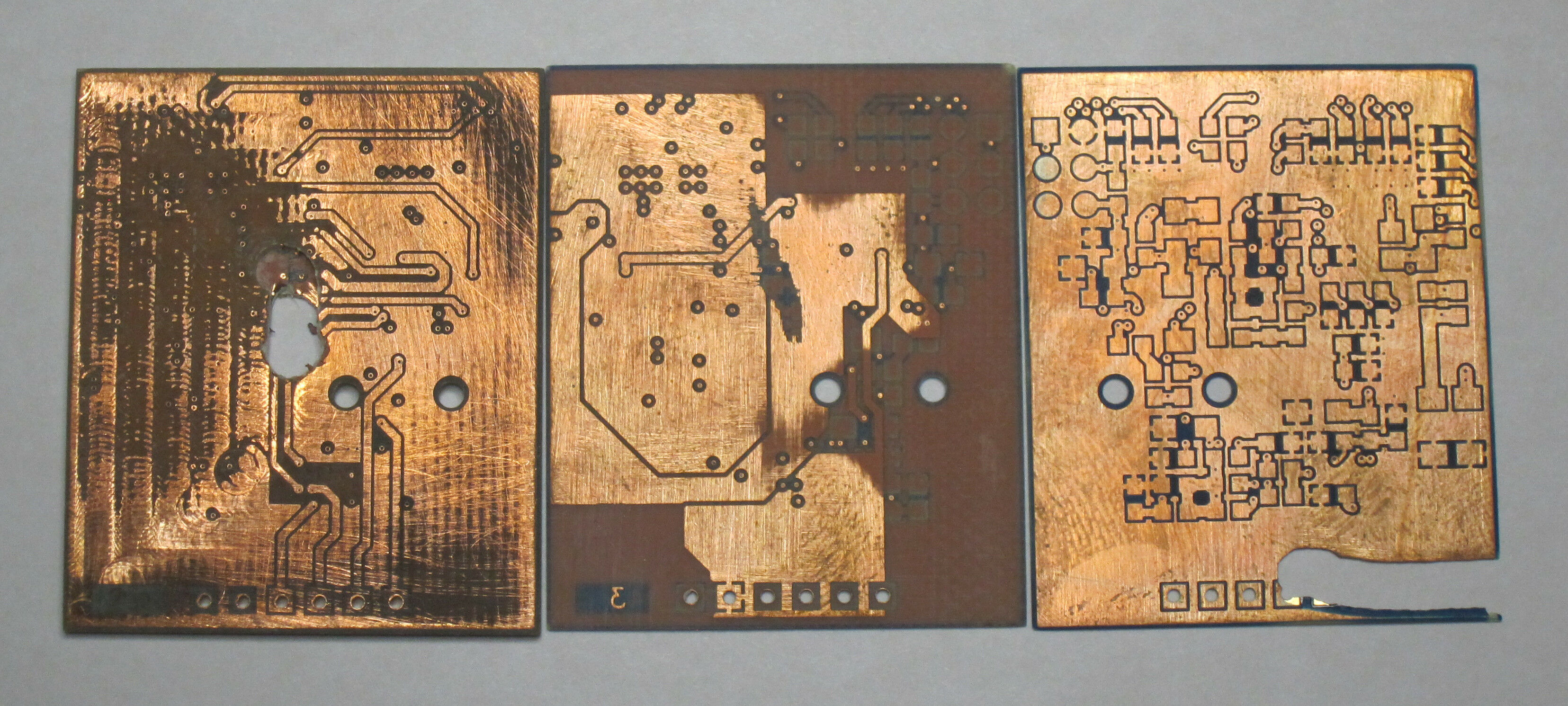
EMIC 2 PCBs damaged during milling and finishing.
The Name Plate
Each encapsulated PCB display contains a small copper name plate. This plate lists some information about the PCB, which layers are in the display, etc. The plates are etched with the same CNC mill, this time using a 60 degree end mill specifically meant for engraving copper. The engraved channels were then filled with a black shellac, specifically “dial wax” used in clock making. The plates were all engraved in a single small sheet of copper and then individually cut out. The plates were heated up and the dial wax applied. They were then sanded and polished.
The copper sheet was held down by double-sided sticky tape as opposed to the vacuum table. We found out pretty quickly that the copper sheet was too rigid and too warped to allow for a proper vacuum seat. The tape worked well enough for this process but the overall warping of the copper sheet gave us issues with the engraving.
Issues
The name plates were by far the largest headache. We bought 4 metal engraving end mills and then promptly destroyed 2 of them by having too high of a feed rate and depth of cut. In the end, all of the text is readable, but some of it is incredibly shallow or has very jagged edges from damaged end mills. With the shallow areas, the dial wax was not able to set in place or was almost fully removed when doing the final finishing process. Additionally, one of the plates was milled out to have the wrong text. I opted to (poorly) redact and replace the text rather than starting over. The text was hammered out with a punch, some solder applied, sanded, and a transparency was glued over top to correct the text. In retrospect, it would have been cleaner to have gently sanded away the incorrect text and then add the transparency on top of that.
Overall, it had a lot of the same problems as the PCBs did, but, the plates required far more precision to do the engraving. Again, using a smaller mill designed for this type of work would have allowed for more precise operation.
Encapsulation
And now, we put it all together. We used silicone moulds that were designed for making drink coasters; ~3.8” x ~3.8” with rounded corners. A two-part clear resin by the name of Amazing Clear Cast was used for the encapsulation process.
Amazing Clear Cast has a set time of about 10 hours with a cure time of 24 hours. This slow process is perfect for encapsulating PCBs. A small layer was mixed and poured in to the mould and left to cure for 6-8 hours. At this stage the layer is slightly gummy. This allows items to be placed on top of it and another layer poured. Amazing Clear Cast actually recommends this 6-8 hour mark for adding another layer as the two layers will still be able to fuse together making a single layer in the end.
Just before the PCBs and name plates were placed, they were given one final polish sanding. This was to remove any surface oxidation of the copper that may have occurred. Another layer of the resin was mixed and painted on to the PCBs and the name plate before they were placed on top of the first layer. The step of painting on the liquid second layer was to help reduce the amount of trapped air under the object.
Both layer sets were mixed very slowly to reduce the amount of bubbles introduced to the resin. Once the layer was poured, a propane touch was run gently over the surface of the layer. The heat causes bubbles to expand, move to the surface, and pop.
Finishing
After allowing the panels to fully cure, they were popped out of the moulds and then finished. The top layer was not perfectly square due to the surface not being completely level. All faces were sanded down to be square and then polished. This process started with 250 grit sandpaper and slowly worked all the way to 3000 grit before having an application of Novus plastic polish.
The result of the finishing is quite amazing. It allows one to see in the edges and observe just how thick the PCB ends up being when it is just two layers. The EMIC 2 display has a full PCB contained in the panel alongside layers 1 & 2, and 3 & 4; which shows just how small the actual signal layers are compared to the finished PCB.
Issues
While a majority of the air bubbles were eliminated, some still exist. Using a pressure pot or taking the time to first vacuum the mixed resin would have helped with this. There are a few unfortunate spots where air was trapped under the PCB or name plate after it was painted and set down on the first resin layer. This is preferred to having the objects sink to the bottom or float to the top. Using the separate layers allowed them to anchor to the first layer more readily. But, overall, I’m quite pleased with this process.
Final Notes
Overall, not counting the original test pieces or cure time of the resin, each panel took roughly 20-25 hours from start to finish. Most of that was in sanding and polishing the delicate copper sheets and the resin plates themselves.
Photos (and more descriptions!)
EMIC 2
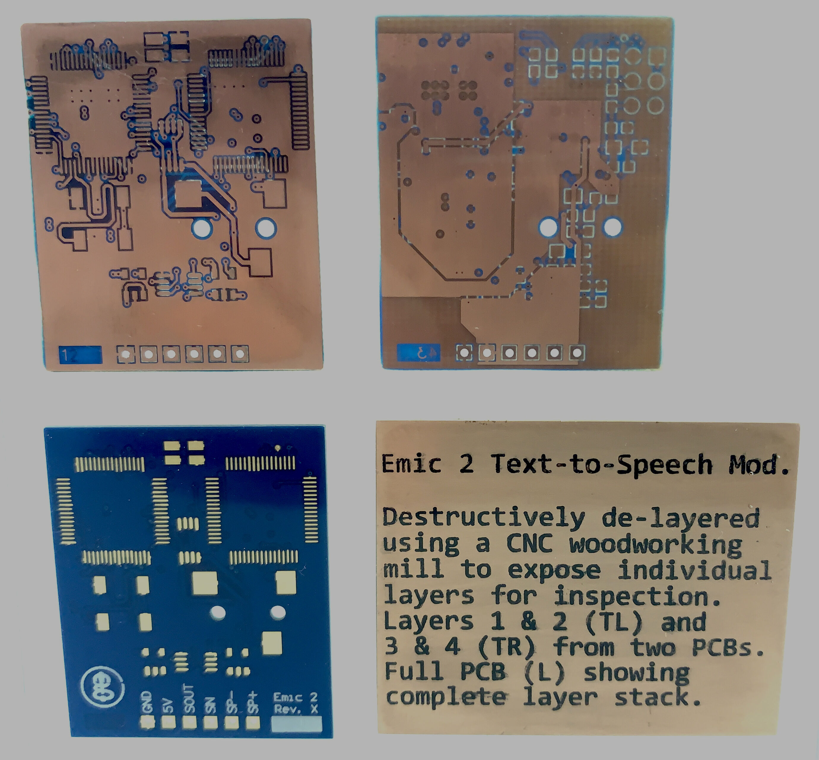
EMIC 2 front side of the panel. This shows layer 1 on the top left (and bottom left), with layer 3 on the top right. Layer 2 is behind layer 1; with layer 4 behind 3. Notice in the bottom left corner of both PCBs is a copper number indicating the layer number. Notice that the “3” is backwards. On the rear side (below) the “4” and “3” numbers are the correct way around. While the whole PCB is designed to look top down through the layers in order 1-4, the layer designators are likely done the way they are so that each layer pair can be verified from the nearest perspective. Its possible to see “1” and “2” from the front but the opacity of the fiberglass means that only “3” and “4” can be seen while looking from the back.
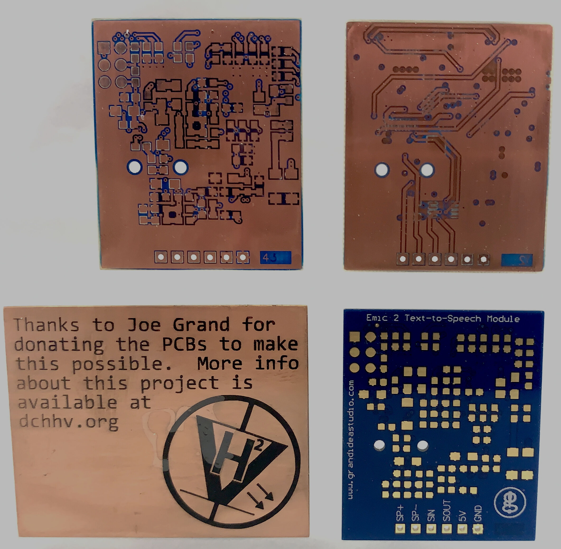
The air bubble around the logo and text on the copper plate was due to a bad placement, unfortunately.
RFID read/write

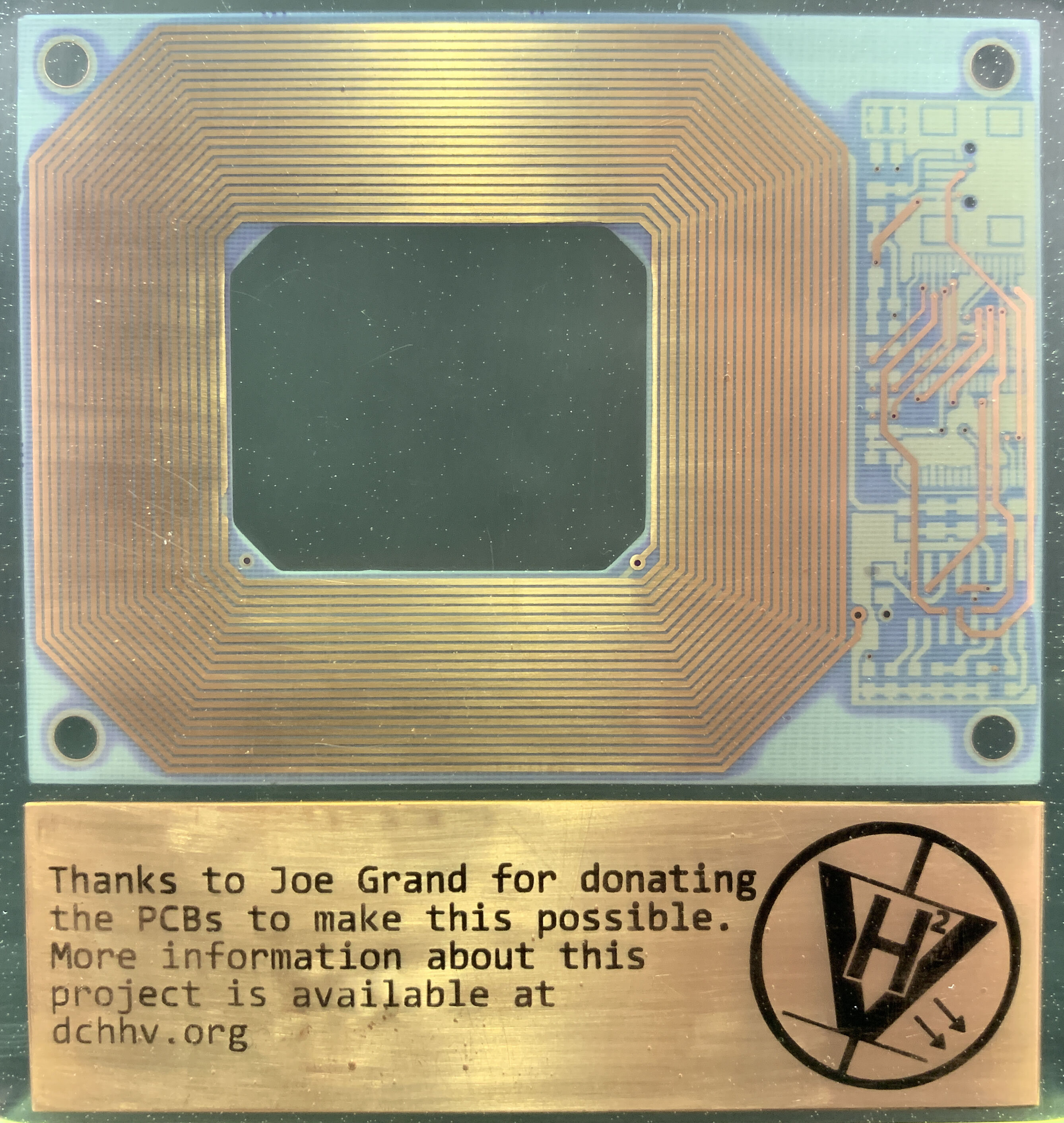
RFID read/write module, layers 1 and 2, front side. This perspective shows layer one. This is an interesting specimen for a couple of reasons. The first is that this actually has a manufacturing defect on the PCB. Take a close look on the right side, in the middle, the 7th trace from the inside edge. There is a weird looking copper blob that extends to the right of the trace and is very close proximity to the trace next to it. This defect highlights why trace/space width as well as manufacturing tolerance is incredibly important when manufacturing PCBs. Additionally, this is the name plate that had a typo. It originally listed layers “3 & 4” (two copies of the same name plate were made). It certainly doesn’t look pretty, but it has character. Also, the engraving channels were very shallow here due to a damaged end mill, our last end mill. See the image below for more.
The rear side of this panel, layer 2, has a defect we introduced during the final de-layering process. On the left side, lower-middle, the innermost trace, its possible to see said trace missing about 1 mm of copper. At this overall thickness (~10 mils), the whole thing is as flexible as a sheet of paper. This makes it very difficult to control pressure or the sanding to get an even finish.
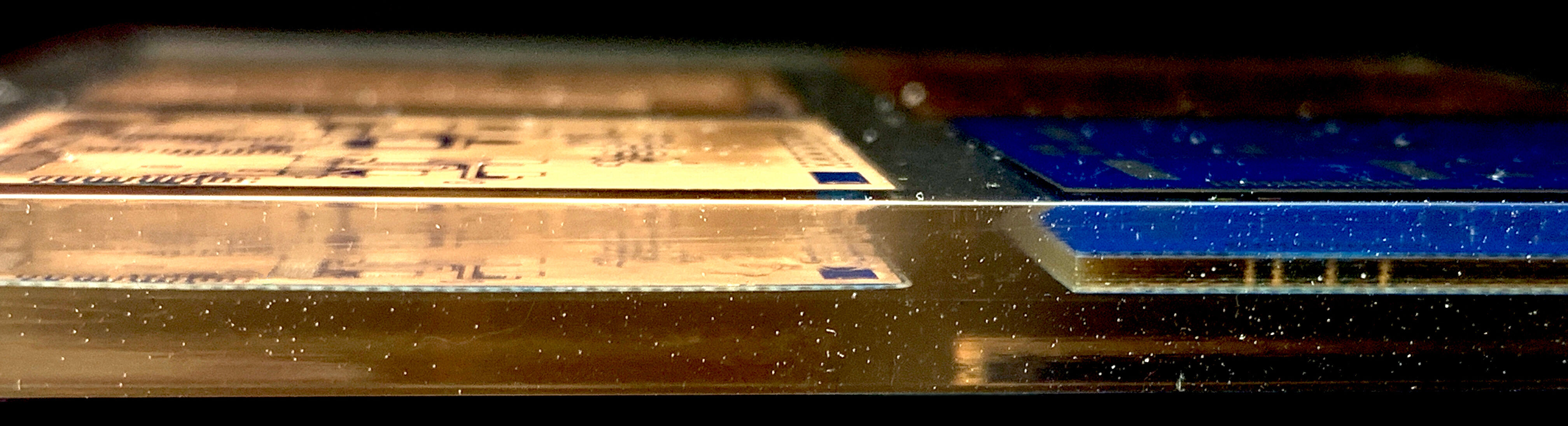
EMIC 2 Side
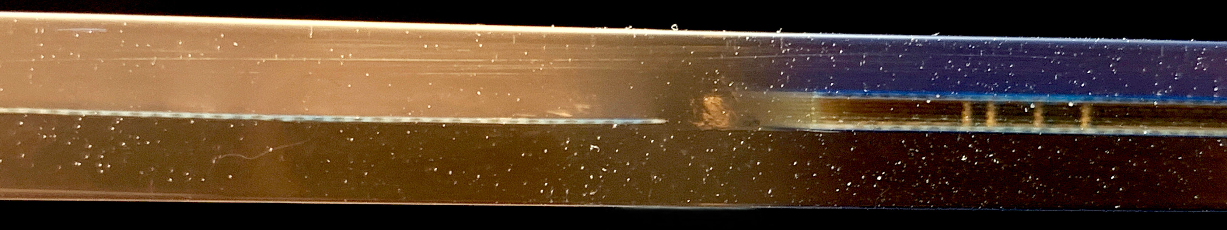
Saved the best for last! This closeup of the edge of the EMIC 2 panel shows some amazing perspectives. On the left side, the thin sheet is actually layers 1 & 2; on the right is the full PCB stackup. Looking at the right side, its now possible to see roughly how the stackup works. The middle area is the larger PCB core. The almost invisible substrate between the top and bottom layer pairs is the prepreg material. Through the core, one can see the plated copper vias connecting signals between all 4 layers (I don’t think this uses blind/buried vias). Most of the “flecks” that can be observed are actually really small trapped air bubbles. They appear so numerous because they are not all on the surface and are visible a few inches deep from this angle.
Next time you find yourself looking at a PCB, take a close look at the edge. You may be able to deduce how many layers they are and the average substrate thickness.